- 您现在的位置:买卖IC网 > Sheet目录2010 > MAX5365EUT+T (Maxim Integrated Products)IC DAC 6BIT LP 3WIRE SER SOT23-6
MAX5363/MAX5364/MAX5365
Low-Cost, Low-Power, 6-Bit DACs with 3-Wire
Serial Interface in SOT23
2
_______________________________________________________________________________________
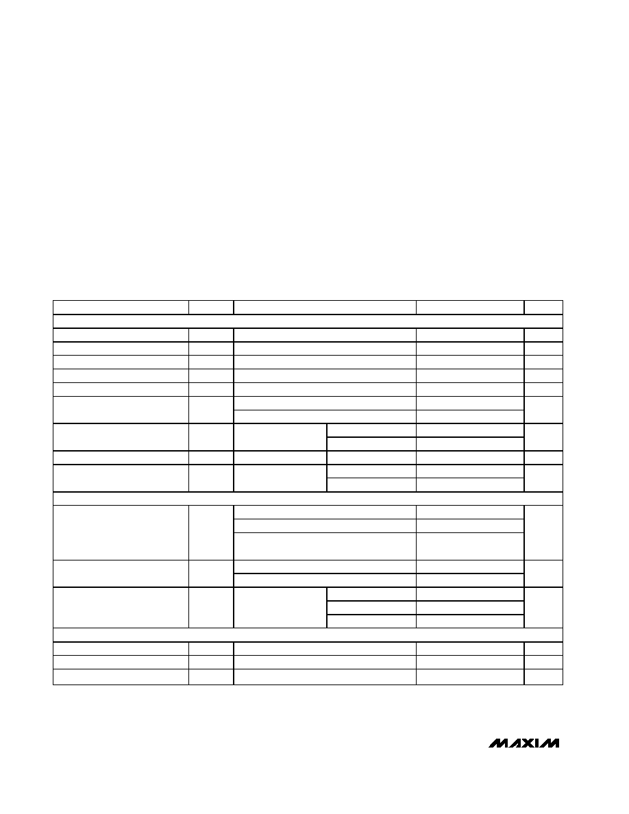
ABSOLUTE MAXIMUM RATINGS
ELECTRICAL CHARACTERISTICS
(VDD = +2.7V to +3.6V (MAX5363), VDD = +4.5V to +5.5V (MAX5364), VDD = +2.7V to +5.5V (MAX5365), RL = 10k
, CL = 50pF, TA =
TMIN to TMAX, unless otherwise noted. Typical values are TA = +25°C.)
Stresses beyond those listed under “Absolute Maximum Ratings” may cause permanent damage to the device. These are stress ratings only, and functional
operation of the device at these or any other conditions beyond those indicated in the operational sections of the specifications is not implied. Exposure to
absolute maximum rating conditions for extended periods may affect device reliability.
VDD to GND ..............................................................-0.3V to +6V
OUT ............................................................-0.3V to (VDD + 0.3V)
CS, SCLK, DIN to GND ............................................-0.3V to +6V
Maximum Current into Any Pin............................................50mA
Continuous Power Dissipation (TA = +70°C)
6-Pin SOT23 (derate 8.7mW/°C above +70°C)...........696mW
Operating Temperature Range ...........................-40°C to +85°C
Storage Temperature Range .............................-65°C to +150°C
Maximum Junction Temperature .....................................+150°C
Lead Temperature (soldering, 10s) .................................+300°C
PARAMETER
SYMBOL
CONDITIONS
MIN
TYP
MAX
UNITS
STATIC ACCURACY
Resolution
6
Bits
Integral Linearity Error
INL
(Note 1)
±1
LSB
Differential Linearity Error
DNL
Guaranteed monotonic
±1
LSB
Offset Error
VOS
(Note 2)
±1
±25
mV
Offset Error Supply Rejection
MAX5365 (Notes 2, 3)
60
dB
MAX5363/MAX5364
3
Offset Error
Temperature Coefficient
MAX5365
1
ppm/
°C
MAX5363/MAX5364
10
Full-Scale Error
Code = 63, no load
MAX5365
5
% of ideal
FS
Full-Scale Error Supply
Code = 63 (Note 4)
MAX5363/MAX5364
50
dB
MAX5363/MAX5364
±40
Full-Scale Error Temperature
Coefficient
Code = 63
MAX5365
±10
ppm/
°C
DAC OUTPUT
MAX5363
1.8
2
2.2
MAX5364
3.6
4
4.4
Internal Reference Voltage
(Note 5)
REF
MAX5365
0.85
×
VDD
0.9
×
VDD
0.95
×
VDD
V
Code = 63, 0 to 100
A
0.5
Output Load Regulation
Code = 0, 0 to 100
A
0.5
LSB
[D13, D12] = 0, 1
1k
[D13, D12] = 1, 0
100k
Shutdown Output Resistance
to GND
VOUT = 0 to VDD
[D13, D12] = 1, 1
1M
DYNAMIC PERFORMANCE
Voltage Output Slew Rate
Positive and negative
0.4
V/
s
Output Settling Time
To 1/2 LSB, 50k
and 50pF load (Note 6)
20
s
Digital Feedthrough
Code = 0, all digital inputs from 0 to VDD
2
nVs
发布紧急采购,3分钟左右您将得到回复。
相关PDF资料
MAX536BEWE+
IC DAC 12BIT QUAD CALIB 16-SOIC
MAX5380NEUK+T
IC DAC 8BIT 2WIRE SER SOT23-5
MAX5384EZT+T
IC DAC 8BIT 3WIRE SER TSOT23-6
MAX541AESA+
IC DAC 16BIT SER/VOLT I/O 8-SOIC
MAX5444AEUB+
IC DAC 16BIT 3V SERIAL 10-UMAX
MAX547BEMH+
IC DAC 13BIT OCTAL PAR 44-MQFP
MAX5480AEEE+T
IC DAC 8BIT PARALLEL 16-QSOP
MAX5511ETC+T
IC DAC 8BIT VOUT 12-TQFN-EP
相关代理商/技术参数
MAX5365EUT-T
功能描述:数模转换器- DAC RoHS:否 制造商:Texas Instruments 转换器数量:1 DAC 输出端数量:1 转换速率:2 MSPs 分辨率:16 bit 接口类型:QSPI, SPI, Serial (3-Wire, Microwire) 稳定时间:1 us 最大工作温度:+ 85 C 安装风格:SMD/SMT 封装 / 箱体:SOIC-14 封装:Tube
MAX536ACPE
功能描述:数模转换器- DAC RoHS:否 制造商:Texas Instruments 转换器数量:1 DAC 输出端数量:1 转换速率:2 MSPs 分辨率:16 bit 接口类型:QSPI, SPI, Serial (3-Wire, Microwire) 稳定时间:1 us 最大工作温度:+ 85 C 安装风格:SMD/SMT 封装 / 箱体:SOIC-14 封装:Tube
MAX536ACPE+
功能描述:数模转换器- DAC 12-Bit 4Ch Precision DAC RoHS:否 制造商:Texas Instruments 转换器数量:1 DAC 输出端数量:1 转换速率:2 MSPs 分辨率:16 bit 接口类型:QSPI, SPI, Serial (3-Wire, Microwire) 稳定时间:1 us 最大工作温度:+ 85 C 安装风格:SMD/SMT 封装 / 箱体:SOIC-14 封装:Tube
MAX536ACWE
功能描述:数模转换器- DAC RoHS:否 制造商:Texas Instruments 转换器数量:1 DAC 输出端数量:1 转换速率:2 MSPs 分辨率:16 bit 接口类型:QSPI, SPI, Serial (3-Wire, Microwire) 稳定时间:1 us 最大工作温度:+ 85 C 安装风格:SMD/SMT 封装 / 箱体:SOIC-14 封装:Tube
MAX536ACWE+
功能描述:数模转换器- DAC 12-Bit 4Ch Precision DAC RoHS:否 制造商:Texas Instruments 转换器数量:1 DAC 输出端数量:1 转换速率:2 MSPs 分辨率:16 bit 接口类型:QSPI, SPI, Serial (3-Wire, Microwire) 稳定时间:1 us 最大工作温度:+ 85 C 安装风格:SMD/SMT 封装 / 箱体:SOIC-14 封装:Tube
MAX536ACWE+T
功能描述:数模转换器- DAC 12-Bit 4Ch Precision DAC RoHS:否 制造商:Texas Instruments 转换器数量:1 DAC 输出端数量:1 转换速率:2 MSPs 分辨率:16 bit 接口类型:QSPI, SPI, Serial (3-Wire, Microwire) 稳定时间:1 us 最大工作温度:+ 85 C 安装风格:SMD/SMT 封装 / 箱体:SOIC-14 封装:Tube
MAX536ACWE-T
功能描述:数模转换器- DAC RoHS:否 制造商:Texas Instruments 转换器数量:1 DAC 输出端数量:1 转换速率:2 MSPs 分辨率:16 bit 接口类型:QSPI, SPI, Serial (3-Wire, Microwire) 稳定时间:1 us 最大工作温度:+ 85 C 安装风格:SMD/SMT 封装 / 箱体:SOIC-14 封装:Tube
MAX536AEPE
功能描述:数模转换器- DAC RoHS:否 制造商:Texas Instruments 转换器数量:1 DAC 输出端数量:1 转换速率:2 MSPs 分辨率:16 bit 接口类型:QSPI, SPI, Serial (3-Wire, Microwire) 稳定时间:1 us 最大工作温度:+ 85 C 安装风格:SMD/SMT 封装 / 箱体:SOIC-14 封装:Tube